- 您现在的位置:买卖IC网 > Sheet目录1993 > DS1374C-3# (Maxim Integrated Products)IC RTC I2C W/CHARGER 16-SOIC
DS1374
I2C, 32-Bit Binary Counter Watchdog RTC with
Trickle Charger and Reset Input/Output
2
_____________________________________________________________________
ABSOLUTE MAXIMUM RATINGS
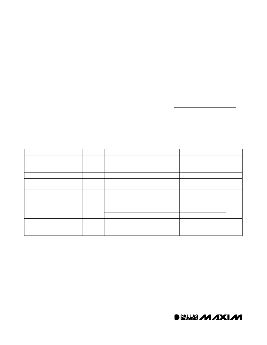
RECOMMENDED DC OPERATING CONDITIONS
(VCC = VCC(MIN) to VCC(MAX), TA = -40°C to +85°C, unless otherwise noted.) (Note 2)
Stresses beyond those listed under “Absolute Maximum Ratings” may cause permanent damage to the device. These are stress ratings only, and functional
operation of the device at these or any other conditions beyond those indicated in the operational sections of the specifications is not implied. Exposure to
absolute maximum rating conditions for extended periods may affect device reliability.
Voltage Range on VCC Pin Relative to Ground .....-0.3V to +6.0V
Voltage Range on SDA or SCL
Relative to Ground ....................................-0.3V to VCC + 0.3V
Junction-to-Ambient Thermal Resistance (
θJA) (Note 1)
16-Pin SO .....................................................................73°C/W
10-Pin SOP ...............................................................221°C/W
Junction-to-Case Thermal Resistance (
θJC) (Note 1)
16-Pin SO .....................................................................23°C/W
10-Pin SOP .................................................................39°C/W
Operating Temperature Range ...........................-40
°C to +85°C
Storage Temperature Range .............................-55
°C to +125°C
Lead Temperature (soldering, 10s) .................................+260
°C
Soldering Temperature (reflow) .......................................+260°C
PARAMETER
SYMBOL
CONDITIONS
MIN
TYP
MAX
UNITS
DS1374-33
2.97
3.3
5.50
DS1374-3
2.7
3.0
3.3
Supply Voltage
(Notes 3, 4)
VCC
DS1374-18
1.71
1.8
1.89
V
Input Logic 1
VIH
(Note 3)
0.7 x VCC
VCC + 0.3
V
Input Logic 0
VIL
(Note 3)
-0.3
+0.3 x
VCC
V
Pullup Resistor Voltage (INT,
SQW, SDA, SCL), VCC = 0V
VPU
(Note 3)
5.5
V
DS1374-33
2.70
2.88
2.97
DS1374-3
2.45
2.6
2.7
Power-Fail Voltage
(Note 3)
VPF
DS1374-18
1.51
1.6
1.71
V
DS1374-33
1.3
3.0
VCC
(MAX)
Backup Supply Voltage
(Notes 3, 4, 5)
VBACKUP
DS1374-3, DS1374-18
1.3
3.0
3.7
V
Note 1:
Package thermal resistances were obtained using the method described in JEDEC specification JESD51-7, using a four-
layer board. For detailed information on package thermal considerations, refer to www.maxim-ic.com/thermal-tutorial.
发布紧急采购,3分钟左右您将得到回复。
相关PDF资料
DS1375T+
IC RTC SERIAL W/ALARM 6-TDFN
DS1384FP-12+
IC CTRLR RTC WDOG 120NS 44-MQFP
DS1386P-8-120+
IC TIMEKEEPER RAM 64K 34-PCM
DS1388Z-3+T&R
IC RTC I2C W/CHARGER 8-SOIC
DS1391U-3+
IC RTC W/CHARGER 10-USOP
DS1394U-33+T&R
IC RTC SPI 3WIRE W/CHRGR 10-MSOP
DS14285SN+T&R
IC RTC W/NV RAM CNTRL 24-SOIC
DS1486P-120+
IC TIMEKEEPER RAM 1MB 34-PCM
相关代理商/技术参数
DS1374C-3#T&R
制造商:Maxim Integrated Products 功能描述:2-WIRE ETC W/CRYSTAL 3V ROHS T/R - Tape and Reel 制造商:Maxim Integrated Products 功能描述:IC RTC I2C 32BIT 3.0V 16-SOIC 制造商:Maxim Integrated Products 功能描述:Real Time Clock I2C 32-Bit Binary Counter Watchdog
DS1374C-3#T&R
功能描述:实时时钟 I2C 32-Bit Binary Counter Watchdog RoHS:否 制造商:Microchip Technology 功能:Clock, Calendar. Alarm RTC 总线接口:I2C 日期格式:DW:DM:M:Y 时间格式:HH:MM:SS RTC 存储容量:64 B 电源电压-最大:5.5 V 电源电压-最小:1.8 V 最大工作温度:+ 85 C 最小工作温度: 安装风格:Through Hole 封装 / 箱体:PDIP-8 封装:Tube
DS1374C-33
功能描述:实时时钟 RoHS:否 制造商:Microchip Technology 功能:Clock, Calendar. Alarm RTC 总线接口:I2C 日期格式:DW:DM:M:Y 时间格式:HH:MM:SS RTC 存储容量:64 B 电源电压-最大:5.5 V 电源电压-最小:1.8 V 最大工作温度:+ 85 C 最小工作温度: 安装风格:Through Hole 封装 / 箱体:PDIP-8 封装:Tube
DS1374C-33-
制造商:MAXIM 制造商全称:Maxim Integrated Products 功能描述:I2C, 32-Bit Binary Counter Watchdog RTC with Trickle Charger and Reset Input/Output
DS1374C-33#
功能描述:实时时钟 I2C 32-Bit Binary Counter Watchdog RoHS:否 制造商:Microchip Technology 功能:Clock, Calendar. Alarm RTC 总线接口:I2C 日期格式:DW:DM:M:Y 时间格式:HH:MM:SS RTC 存储容量:64 B 电源电压-最大:5.5 V 电源电压-最小:1.8 V 最大工作温度:+ 85 C 最小工作温度: 安装风格:Through Hole 封装 / 箱体:PDIP-8 封装:Tube
DS1374C-33##
制造商:Maxim Integrated Products 功能描述:
DS1374C-33#
制造商:Maxim Integrated Products 功能描述:IC RTC BINARY SOIC-16
DS1374C-33#T&R
制造商:Maxim Integrated Products 功能描述:I2C 32-BIT BINARY COUNTER WATCHDOG RTC 制造商:Maxim Integrated Products 功能描述:REAL TIME CLOCK SERL 16SOIC W - Tape and Reel 制造商:Maxim Integrated Products 功能描述:IC RTC I2C W/CHARGER 16-SOIC 制造商:Maxim Integrated Products 功能描述:Real Time Clock I2C 32-Bit Binary Counter Watchdog